Technology of double sided printed wiring boards
|
1. |
Copper clad laminate:  |
|
- substrate thicknesses: 0.2, 0.25, 0.4, 0.5, 0.8, 1.0, 1.2, 1.55, 2.0, 2.5 mm
- copper layer thicknesses: 18, 35 µm
|
|
|
2. |
Stacking, drilling, brushing:  |
|
- range of hole diameter: 0.3–6.3 mm in 100 µm steps
- average positional offset: 50 µm
|
|
|
3. |
Plating through-holes (making the hole walls conductive):  |
|
- DOW chemicals
- CRIMSON direct electroplating
|
|
|
4. |
Laminating photosensitive dry film:  |
|
- DuPont Riston
- thickness: 38 µm
|
|
|
5. |
Exposure and developing the resist:  |
|
|
|
|
6. |
Electroplating copper:  |
|
|
|
|
7. |
Electroplating tin – positive mask:  |
|
|
|
|
8. |
Stripping the photoresist mask:  |
|
|
|
|
9. |
Selective etching:  |
|
- MacDermid (alkaline etchant solution)
|
|
Double-sided printed wiring boards with plated through-holes, electroplated tin surface finish Recommended for hand soldering |
Double-sided printed wiring boards with plated through-holes, selective chemical surface finish Recommended for reflow and wave soldering |
10. |
Printing photosensitive solder mask and legend:  |
10. |
Stripping tin:
 |
- colours: green, white, black, blue, red, yellow
|
- MacDermid (acid stripper)
|
11. |
Exposure by UV light, developing:
 |
11. |
Printing photosensitive solder mask and legend:  |
|
|
- colours: green, white, black, blue, red, yellow
|
|
|
12. |
Exposure by UV light, developing:  |
|
|
|
|
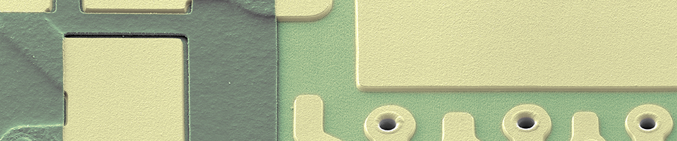
13. |
Protecting solder pads:  |
|
- selective, immersion silver finish
- thickness: 0.5 µm
|
|